In the Internet-of-Things (IoT) era, ubiquitous smart sensing systems significantly contribute to the Big Data paradigm and they are gradually incorporating some sort of edge computing. Such smart sensing applications demand low-power analog-to-digital converters (ADCs) featuring high resolution, with signal-to-noise-and-distortion ratio (SNDR) figures as high as 90dB, but with practical bandwidth values typically not exceeding the kHz range. Oversampling Delta-Sigma modulators (DSMs) are well suited for these requirements, and their switched-capacitor (SC) circuit implementations usually show higher robustness against CMOS technology variations than their continuous-time counterparts. However, the number of fabricated SC DSMs with SNDR > 90dB and bandwidth values exceeding 20kHz is relatively scarce [1]. Indeed, these high-resolution general-purpose data converters are not usually setting the absolute state-of-art Schreier figure of merit FOMS = SNDR + 10*log(Sampling frequency/Power consumption). In practice, their CMOS circuit implementations must face complex design aspects, such as flicker noise, switch non-linearity and charge injection, technology mismatching, OpAmp gain non-linearity, clock jitter or noise coupling through supplies, among others. Even the FOMS value alone cannot take into account critical issues as robustness against technology and temperature, the need for circuit calibration or the use of supply bootstrapping to drive the SC switches.
In the above design context, several DSM architectural strategies have been employed in order to improve dynamic range: high-order (>4) single-loop noise shaping, which is prone to instability; multi-stage noise shaping (MASH) that tends to suffer from technology mismatching at the reconstruction filtering; and SAR-driven Zoom DSMs, whose internal full-scale control introduces glitches and excess of out-of-band harmonics. At CMOS circuit level, flicker noise contributions in the kHz range are commonly attenuated in fully differential topologies by the use of chopping despite the resulting ripple and harmonics.
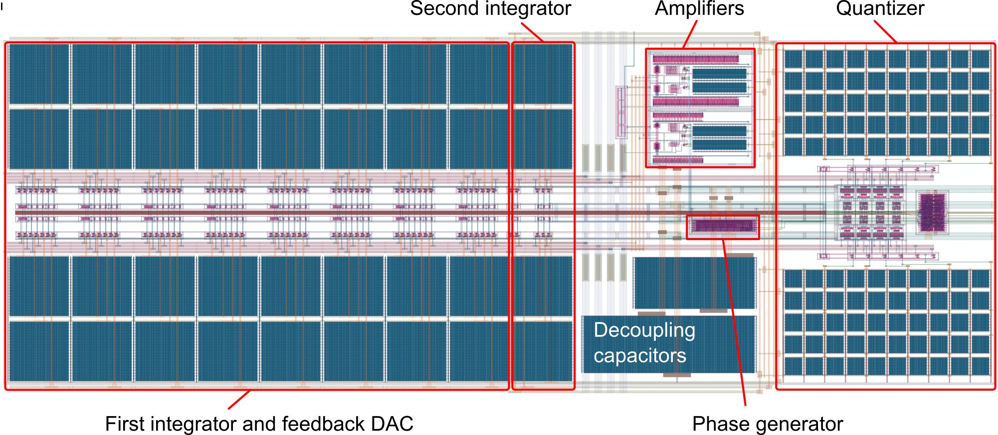
The proposed low-power high-resolution ADC IP is based on a 9-level second-order SC DSM exceeding 90-dB peak SNDR, with 50-kHz bandwidth and a built-in flicker noise cancellation based on correlated double sampling (CDS). The DSM CMOS circuits incorporate switched Class-AB variable-mirror OpAmps (VMAs), which avoid both 50% of static power and the use of switch bootstrapping, together with a SC multi-bit flash quantizer. Compared to state-of-art single-loop SC DSMs, the improvement in power efficiency translates into an increase of 6dB to 12dB in FOMS. Also, the presented 1/f noise cancellation does not cause the typical ripple and harmonics of chopping solutions. Unlike Zoom DSMs, this modulator does not generate excess of harmonics and it features a high spectral purity for input amplitudes close to the full scale.

The IP block includes the DSM itself together with the digital decimator for downsampling close to Nyquist rate and a standard AXI Lite backend (not shown in Picture 1). Thanks to the combination of multi-bit quantization, low shaping order and moderate oversampling, the ADC IP saves about 75% of the power associated with internal signal dynamics compared to equivalent single-bit DSMs. Also, the CDS flicker noise cancellation mechanism allows a net improvement of 10dB in FOMS. At CMOS circuit level, the use of VMAs translates into a low sensitivity to both process and temperature corners.
This data converter IP has been ported to three different CMOS technology nodes: XFAB 1.8V 180nm, TSMC 1.2V 65nm and GF 0.8V 22nm. All implementations target 95-dB SNDR and 50-kHz bandwidth running at 12.8MS/s, with power consumption and silicon area downscaling of {741,632,197} µW and {0.202,0.186,0.043} mm2, respectively. The resulting state-of-art FOMS are 176.0dB. 178.8dB and 179.6dB. Currently, the 180-nm IP has been measured [2], the 65-nm version is going to be tested in short and the 22-nm design is ready for its tape out.
[1] B. Murmann, ADC Performance Survey 1997-2021, http://web.stanford.edu/~murmann/adcsurvey.html.
[2] A. Suanes, L. Terés, M. Dei and F. Serra-Graells, A 0.8mW 50kHz 94.6dB-SNDR Bootstrapping-Free SC Delta-Sigma Modulator ADC with Flicker Noise Cancellation, Proceedings of the IEEE International Symposium on Circuits and Systems (ISCAS), pp. 1-5, Daegu, Korea, May 2021, https://doi.org/10.1109/ISCAS51556.2021.9401688