In the DRAC project we are designing SoCs (System-on-Chip) that include processors based on the RISC-V architecture, different accelerators and a set of analog blocks such as a PLL (Phase-Locked Loop), a SerDes (Serializer Deserializer), an ADC (Analog to Digital Converter) and SPADs (Single Photon Avalanche Diode). Of these analog blocks, the PLL and the SerDes allow to increase the number of instructions executed by the processor; the PLL allows to increase the working frequency while the SerDes enables faster communications with the external memories. Moreover, the ADC allows interaction with analog sensors and SPADs are a tool to enable quantum cryptography.
When planning the integration strategy of the different elements of the SoC, it should be considered that we will work with a mixed signal design. However, as the bigger and the most complex circuits are the digital ones, the chosen strategy is the DoT (Digital On Top). This means that we will start to work as if the SoC were purely digital, and halfway we will add the information of the analog blocks that have been designed separately.
Each analog block is designed following the analog flow, using Cadence®'s "virtuoso" tool. On the other hand, digital designs such as the processor or the accelerators are encoded with RTL (Register-Transfer Level) language, which allows us to describe the behavior of the circuit that we want to design and verify it with simulations. Once we are sure that the designed circuit has the expected behavior, the described behavior needs to be translated into a set of logic gates that perform the same function. This step is called logical synthesis; to carry it out, it is necessary to describe our circuit, to add the information about the available gates of the chosen technology, and to include the constrains of the circuit (figure 1).
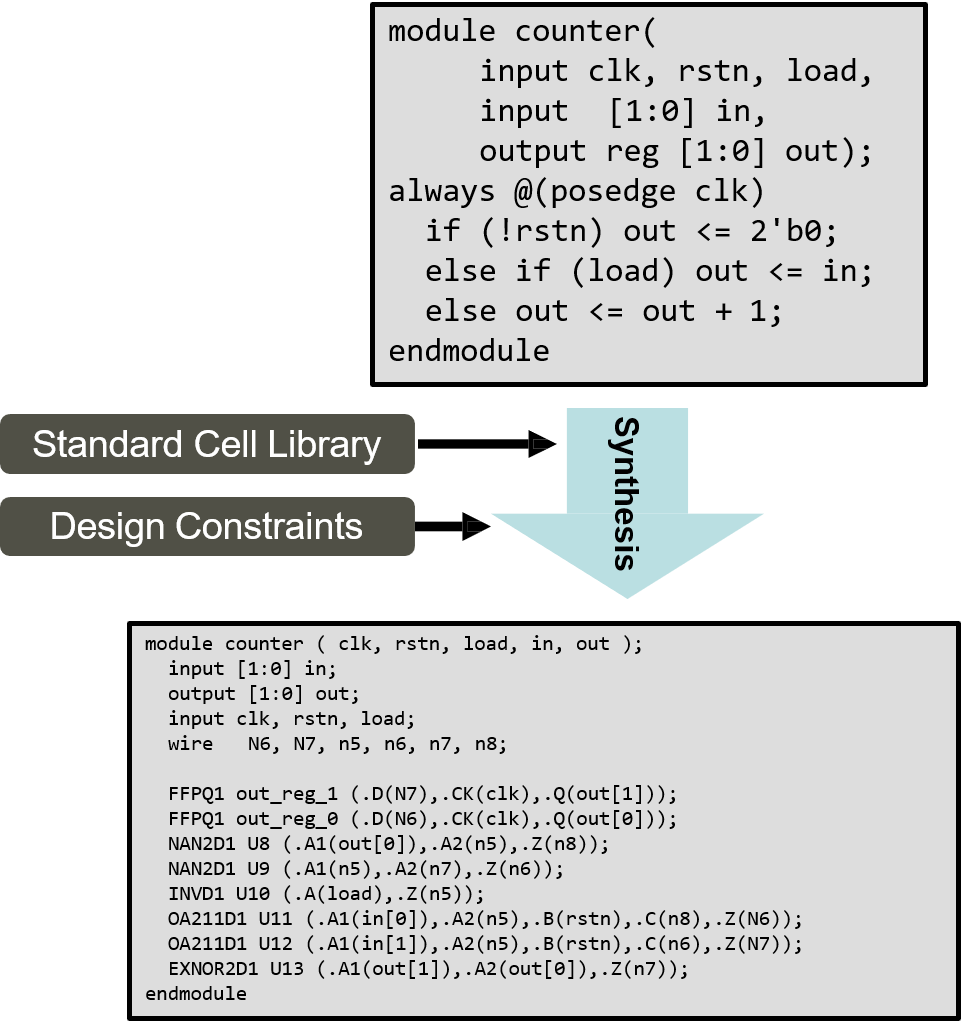
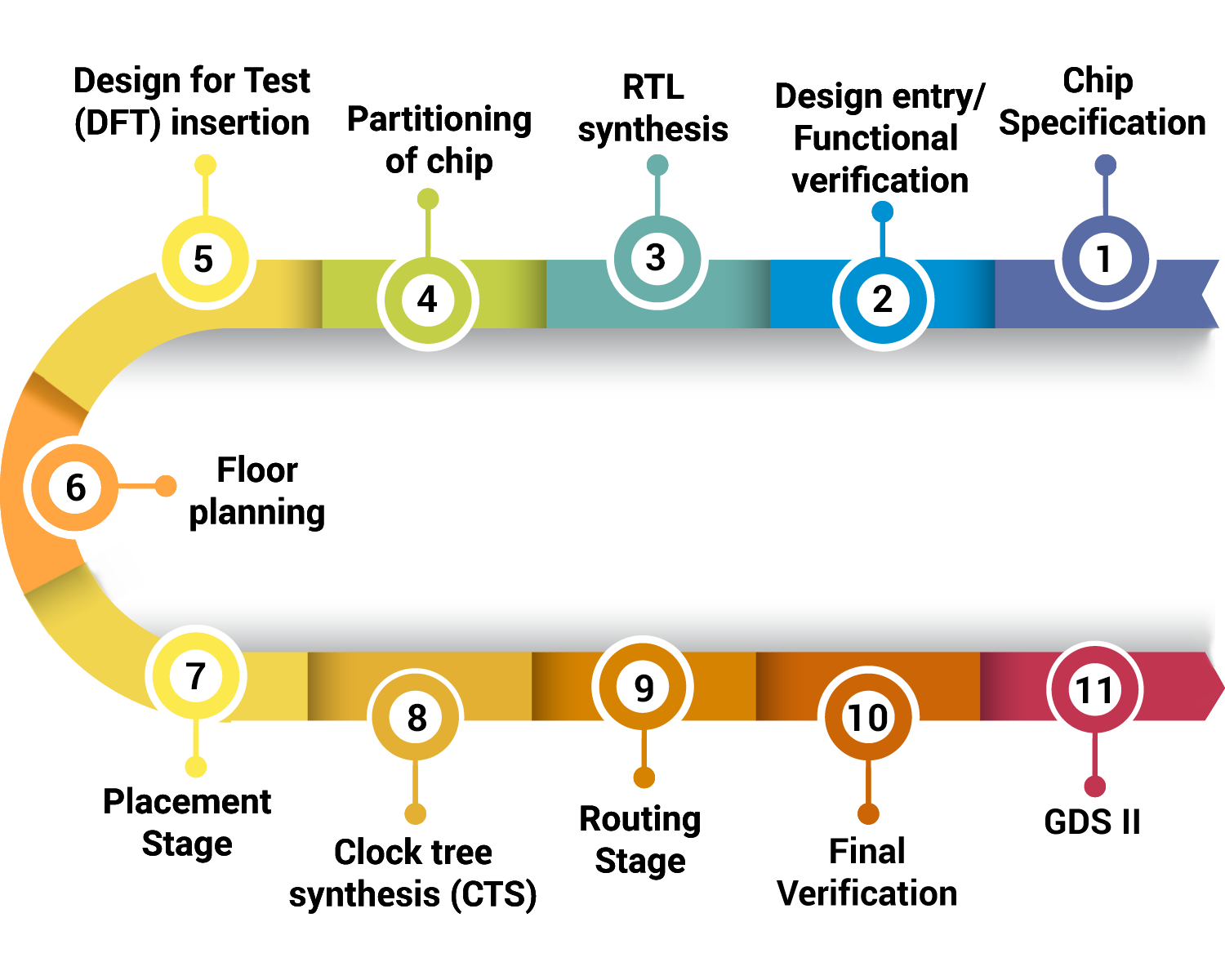
Once the synthesis is finished, we obtain a file, called "netlist", where we will find the digital circuit that we have designed expressed using logic gates available in the chosen technology. The next step consists in distributing the logic cells, analog blocks, GPIOs and memories in a certain area and, in addition, making the connections between them. This step is called physical synthesis, and it can be summarized, very briefly, in 5 stages: Floorplan, Placement, Clock tree synthesis (CTS), Routing and Signoff or Final Verification (see figure 2, steps from 6 to 10).
In the Floorplan stage we make the distribution of our SoC, the area that the digital circuits will use, where we are going to place the memories, GPIOs and the analog blocks and how we are going to power the circuits. In the Placement stage, a first arrangement of the logic gates is made to verify that the design can really be implemented, considering the available area and the time constraints that we want to achieve. In the CTS stage, the clock network distribution of the system is implemented. In the Routing stage, the physical connection of the logic gates is made through metal lines. Finally, the Signoff stage serves to close the chip; timing and design rules checks are carried out to find out if the chip meets the timing constraints that we want and if the chip can be manufactured. This stage ends by generating a GDS II file which, in short, is what the semiconductor factory needs to manufacture the chip.

Fig. 2: Simplified flow of the steps needed to design a chip, from the initial idea to the file that will be sent to the foundry. Physical synthesis includes steps 6 to 10. Image taken from: https://www.einfochips.com/blog/asic-design-flow-in-vlsi-engineering-services-a-quick-guide/