
There are different research groups involved in the design of the first chip of the DRAC project (Sargantana). Three of them are from the DRAC project: Barcelona Supercomputing Center (BSC), Universitat Politècnica de Catalunya (UPC) and Universitat de Barcelona (UB). In addition, the Instituto Politécnico Nacional (IPN) of Mexico and the Institute of Microelectronics of Barcelona (IMB-CNM), in particular the ICAS (Integrated Circuits and Systems) group, have also participated in the design.
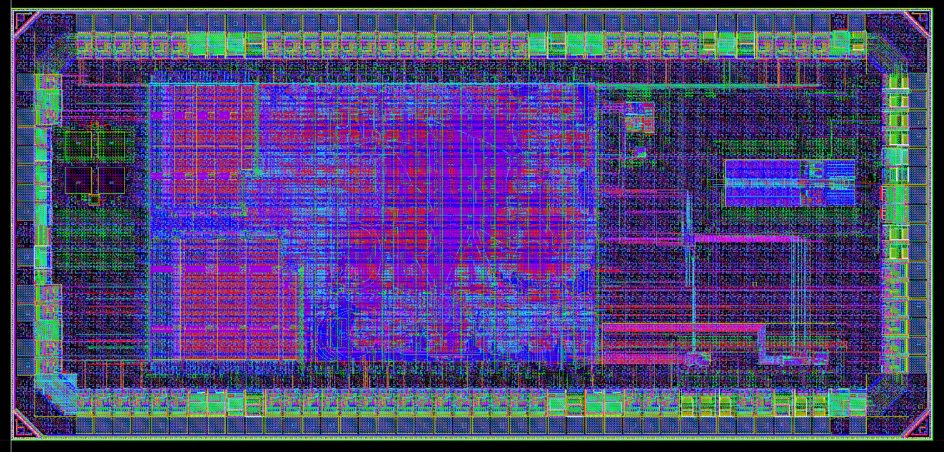
The first chip designed in the project was sent to fabrication on February 18, 2022. The chip is shown in Figure 1a, measures 2.49 mm x 1.17 mm, giving a total area of 2.91 mm2, and it was designed in the GlobalFoundries 22nm technology. Apart from the RISC-V Sargantana processor designed in the project, it contains different designs necessary for the correct operation of the processor. These circuits are shown in Figure 1b.
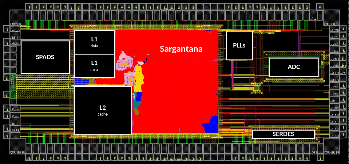
The chip aims to characterize the IPs supplied by Synopsys, such as memories and digital cells, the Sargantana processor and the analog IPs designed by the different groups involved in the project. The contribution of each research group to the chip (Figure 1b) is detailed below:
Sargantana: RISC-V processor, designed by BSC and IPN, with a 7-stage pipeline, uses the Instruction Set Architecture (ISA) RV64IMAFD and it contains an integer vector unit for genomics. It includes memories from Synopsys. More details of the processor can be found in the following link.
Phase-locked loop (PLL): A PLL is a circuit to generate a high frequency clock for the processor. Two PLLs have been integrated in this chip, which allows us to have a backup solution in case one of them does not work properly. The PLLs have been designed by the ICAS group of the IMB-CNM and by the UPC, respectively.
SerDes: A SerDes, or serializer/deserializer, is a circuit commonly used in high-frequency communications. This circuit has been designed by the UPC.
Analog/Digital Converter: Design of the ICAS group of the IMB-CNM, previously published in the following link.
SPI configuration block: Digital design of the ICAS group of the IMB-CNM that allows configuring the different analog IPs.
Single Photon Avalanche Diodes (SPADs): SPADs are solid-state photodetectors and can be used to generate random numbers. The design group of the UB integrated a couple of SPAD structures.
Physical synthesis: The physical synthesis of the chip was carried out by the UB, and the steps followed during the place and route (i.e., placing the different elements, routing them and checking that the design meets the design rules from the foundry) are detailed in the following link. After that, two additional steps were performed: Static timing analysis (STA) and power analysis.
For the STA studies, a parasitic model of the chip is created to study if the design meets the timing constraints imposed by the designers. The results show that the processor can work at a frequency of up to 1.4 GHz.
Power analysis studies were performed assuming that the processor has an activity of 10% and checking the static consumption for the best, typical and worst cases at different temperatures. In all these cases, the results show that the power distribution is correct, and the IR drop can be corrected.