
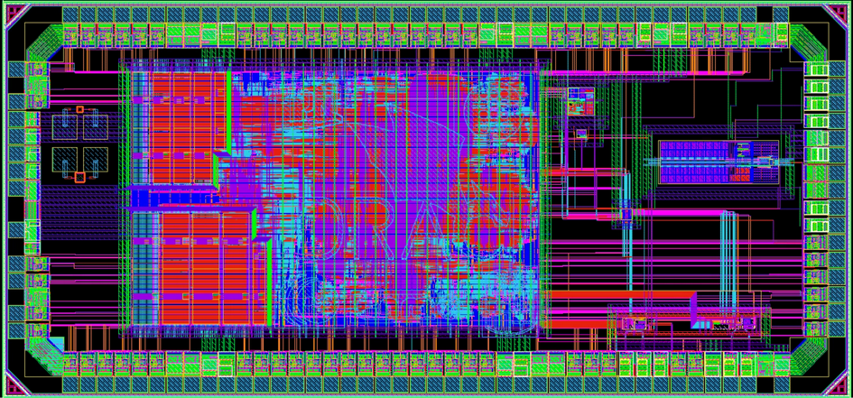
We are pleased to announce that the third generation of the Lagarto processor series has been submitted for fabrication in GlobalFoundries 22nm technology node via Europractice. This design is based on the open source instruction set architecture (ISA) RISC-V and is a design jointly developed by researchers from BSC, CIC-IPN, CNM, UAB, UB, UPC and URV.
This new design is called Sargantana (lizard name in Aragonese and Catalan) and integrates a Lagarto scalar core together with multiple analog IPs. Sargantana is the first fabricated design that breaks the gigahertz frequency wall in the Lagarto series.
Main novelties of Sargantana with respect to DVINO, the second generation of the Lagarto series:
- New in-order core design with an expected 36% IPC improvement with simulated benchmarks.
- Deeper pipeline design to reach 1.2GHz in the typical corner.
- Added support for single and double floating point support (F and D RISC-V extensions).
- Added a new 128-bit SIMD vector processing unit (VPU) for integer and custom genomics vector instructions.
- Non-blocking memory accesses with up to 16 misses in flight (up to 2 cache block misses).
- Added new high speed SerDes memory controller (between 2 and 8 Gbps).
- Added custom bootROM controller.
- Added custom 16-bit high resolution analog-to-digital converter (ADC) IP with flicker noise cancellation and AXI4-Lite standard bus interface.
- Added custom single-photon avalanche diode (SPAD) IP for random number generation.
Sargantana processor details:
- Lagarto Hun scalar pipeline, 7-stage, in-order, RV64IMAFD ISA, privileged ISA 1.11.
- Integer VPU for genomics, 128-bit vector length, vector ISA 0.7.1.
- Integrated on-chip integer Phase Locked Loop (PLL) designed and simulated to run from 600MHz to 2.2GHz.
- In-house L1 instruction cache and PMU (performance monitoring unit).
- L1 data and L2 caches from Untethered lowRISC version 0.2.
- Multiple essential peripheral controllers: JTAG, UART, SPI, bootROM, SerDes and HyperRAM.
- In-house JTAG-based debug-ring.
- Technology node: GF 22nm.
- Area: 2.89mm2.
Processor details of previous generations of Lagarto designs:
- Second generation Lagarto press release (2021): https://drac.bsc.es/en/media/news/tech-dvino-second-generation-lagarto-processor-series-submitted-fabrication-europractice
- First generation Lagarto press release (2019): https://www.bsc.es/news/bsc-news/the-bsc-coordinates-the-manufacture-the-first-open-source-chip-developed-spain