
On February 2022, the Sargantana processor design was sent for manufacturing to Globalfoundries (via Europractice). Once the chip is processed, the next step will be its validation, which will allow us to determine if the final characteristics correspond to the initial specifications. For this purpose, the different chip modules will be accessed through a custom test system composed by a test Printed Circuit Board (PCB) interconnected to a FPGA-based characterization system through a high-speed SERDES bus.
In this post we explain the characteristics of the test PCB, including the study and simulation of the interconnection tracks, to ensure the integrity of the signal, the structure and the number of layers, which allow the reduction of electromagnetic emissions (EMIs), and the reduction of noise in common mode and in differential mode.
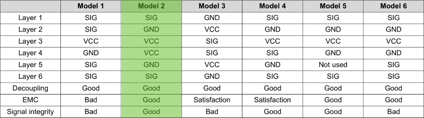
The PCB was designed using the Xpedition Enterprise from Siemens EDA. In addition to schematic and layout entry, Xpedition also allows us to simulate the transmission tracks from the PCB design files, suggesting options that would maximize signal integrity and reduce noise. In particular, we use this property on those lines that connects Sargantana with the memory chips included on the PCB. In addition to these lines, SERDES tracks were also simulated, since these were differential lines that worked at very high speeds. Finally, although initially it was thought to work with a four-layer PCB, it was decided to expand them to 6 to minimize noise and maximize signal integrity. Observing the lines that interconnect the microprocessor with the memory chips and SERDES, an undulation of the tracks can be verified. This type of layout is usual in high-speed circuit systems, as the track layout allows the information transmitted by all lines in parallel to reach its destination at the same time.
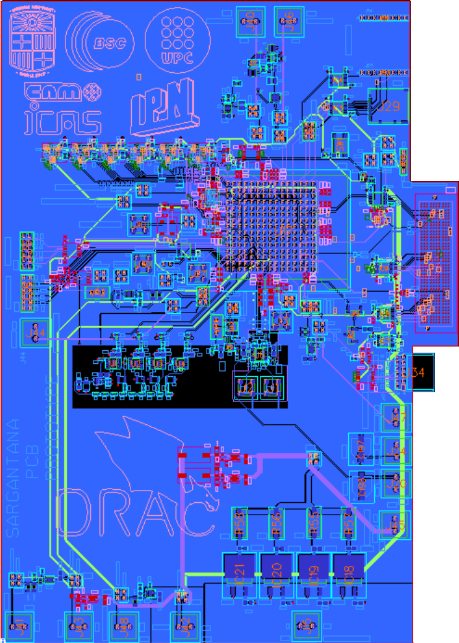
Figure 1 shows the upper layer of the final PCB design sent to be manufactured by our distributor: the company Rompal Ingenieros S.A. Figure 2 shows the chosen layer structure, following the design rules of the Texas Instruments document: High-Speed Layout Guidelines (SCAA082A).
The PCB also allows to supply the complete system. The main supply is a 5V input that generates the 3.3V power supply signals for the different connection interfaces, such as the UART and SPI serial interfaces or the serial programming interface, 2.5V to power the FMC connector on the FPGA board, 1.8V for the HyperRam memories and the I/O processor’s block, and 0.8V for the processor core. The design of the test board also allows us to specifically power each of the power blocks through connectors and using external sources.
The clock system included in the PCB generates the reference signals for processor and ADC. The processor reference oscillator works at a frequency of 100 MHz, while the ADC oscillator works at 26.5 MHz.
In summary, in this post we explain the general characteristics associated with the design of the test PCB developed to characterize the Sargantana chip. The simulations carried out to obtain a correct signal integrity, the track layout characteristics, and some of the most important blocks that make it up have been commented on.