We are pleased to announce that the fourth generation of the Lagarto processor series has been submitted for fabrication in Globalfoundries 22nm technology node via Europractice. This design is based on the open source instruction set architecture (ISA) RISC-V and is a design jointly developed by researchers from BSC, CIC-IPN, CNM, UAB, UB, UPC and URV.
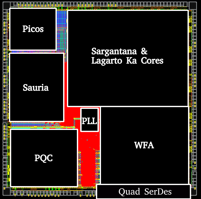
This new design is called Kameleon as it integrates a Lagarto Ka out-of-order core together with multiple domain-specific accelerators. As a result, the Kameleon design can change its color (accelerator) depending on the target application domain.

Main novelties of the Kameleon design with respect to previous generations of the Lagarto series:
-
New out-of-order dual-issue core design to achieve high performance.
-
Includes a second core to achieve energy efficiency based on the Sargantana processor design.
-
Larger L1 and L2 caches for increased capacity and performance.
-
Added SAURIA, a new neural network accelerator for automotive applications based on a systolic array design with approximate computing for high energy efficiency.
-
Added WFAsic, a new accelerator for genomics applications with a custom implementation for the Wavefront Alignment algorithm.
-
Added PQC, a new accelerator for post-quantum cryptography encryption and decryption based on the Classic McEliece scheme.
-
Added PICOS, a new accelerator for hardware task scheduling in the RISC-V processor and accelerators.
-
Added a four-channel high speed SerDes memory controller (between 2 and 8 Gbps).
Kameleon System-on-Chip (SoC) details:
-
Lagarto Ka scalar pipeline, 10-stage, out-of-order, RV64IMA ISA, privileged ISA 1.11.
-
Sargantana scalar pipeline, 7-stage, in-order, RV64IMAFD ISA, privileged ISA 1.11, 128-bit integer VPU for genomics vector ISA 0.7.1.
-
Domain-specific accelerators: SAURIA (automotive), WFAsic (genomics), PQC (security) and PICOS (HW task scheduling)
-
Integrated on-chip integer Phase Locked Loop (PLL) designed and simulated to run from 600MHz to 2.2GHz.
-
In-house L1 instruction cache and PMU (performance monitoring unit).
-
L1 data and L2 caches from Untethered lowRISC version 0.2.
-
Multiple essential peripheral controllers: JTAG, UART, SPI, bootROM, SerDes and HyperRAM.
-
In-house JTAG-based debug-ring.
-
Technology node: GF 22FDX (22nm.)
-
Area: 9.0mm2.
Processor details of previous generations of Lagarto designs:
- Third generation Lagarto press release (2022): https://drac.bsc.es/en/sargantana2
- Second generation Lagarto press release (2021): https://drac.bsc.es/en/media/news/tech-dvino-second-generation-lagarto-processor-series-submitted-fabrication-europractice
- First generation Lagarto press release (2019): https://www.bsc.es/news/bsc-news/the-bsc-coordinates-the-manufacture-the-first-open-source-chip-developed-spain